
Investigating the Effect of Ph Variation on the Optoelectronic and Structural Properties of Electrodeposited Copper Selenide Thin Films.
- O. O. OLUSOLA
- A. I. MUKOLU
- 448-456
- May 23, 2024
- Chemistry
Investigating the Effect of Ph Variation on the Optoelectronic and Structural Properties of Electrodeposited Copper Selenide Thin Films.
O. O. OLUSOLA1*and A. I. MUKOLU2
1Department of Physics, Bamidele Olumilua University of Education Science and Technology, Ikere Ekiti, Nigeria.
2Department of Physics, Ekiti State University, Ado Ekiti, Nigeria.
*Corresponding Author
DOI: https://doi.org/10.51584/IJRIAS.2024.904033
Received: 04 April 2024; Accepted: 17 April 2024; Published: 23 May 2024
ABSTRACT
Copper Selenide (CuSe) thin film compound semiconductors have been deposited onto fluorine doped tin oxide (FTO) conducting substrates using electrodeposition technique through various electrolytic bath pH values of 2.00, 2.20, and 2.40. The deposition was carried out in potentiostatic mode using a 2-electrode system set-up at room temperature for 15 minutes at the cathodic voltage of 500 mV. The electrical and the optical properties of the thin films were carried out using photoelectrochemical (PEC) cells and ultraviolet visible spectrophotometer respectively. CuSe thin film possesses a p-type electrical conductivity and the sample grown at semiconductor and a pH of 2.2 was recorded to have the highest PEC signal and highest photo and dark currents that brings forth its maximum power. The energy band gap values of the electrodeposited CuSe thin films were observed to be 2.30 eV, 2.20 eV, and 2.00 eV at bath pH values of 2.0, 2.2, and 2.4 respectively. The optical band obtained at the various pH decreases as pH increases and these band gap values agree with the bulk band gap of CuSe. The preferred orientation peak of electrodeposited CuSe layers exists as klockmannite (CuSe) and the highest peak intensity for the preferred orientation peak occurred at pH of 2.20. At this pH value, the electrodeposited CuSe layers have the highest crystallite sizes.
Keywords: CuSe, pH variation, electrodeposition technique, electrical, optical, structural,
INTRODUCTION
Copper selenide (CuSe) is a I-VI compound semiconductor that has been studied with great interest in the resent years because of its imminent output in producing optical devices. Copper selenide is a direct band gap p-type semiconductor with an energy band gap value in the range between 2.1 and 2.7 eV, which makes it fascinating for solar energy conversion (Ramesh et al., 2014) (Petrovic et al., 2017). Copper selenide as a metal chalcogenide semiconductor, is a suitable material for many photovoltaic applications due to its excellent electrical and optical properties. It has many structural phases such as orthorhombic (Cu2Se), hexagonal (CuSe) and cubic (Cu2-xSe). it also exist in mineral forms like berzelianite (Cu2Se), umangite (Cu3Se2), klockmannite (CuSe) and naumannite (CuSe2). it has an indirect band gap of 1.4 eV for x = 0.2 (Sandoval-Paz et al., 2016), (Boolchandani et al., 2018), (Ramesh et al., 2014), (Gromboni & Mascaro, 2016). This make the material ennoblement to offer high efficiency of conversion. CuSe thin films have been produced by many researchers through different method among which are: Ramesh et al., 2014, which looked at the optical, morphological, and structural characteristics of thin films of copper selenide using electrodeposition technique. Ezenwa et al., 2013, studied the thin-film copper selenium’s optical properties using chemical bath method, Islam and Bhuiyan 2005., investigated .the structural, electrical, and optical characteristics of copper selenide thin films produced using the chemical bath deposition approach, Guerrero and Nair 1999, examined how heat processing affected the electrical and optical properties of thin films made of copper selenide , Qasrawi & Rob, 2019, investigated the impact of adding aluminium nanosheets to stacked layers of selenium on their structural, optical, and dielectric characteristics. Among other methods used involved vacuum evaporation (Petrović et al., 2017),. The growth of CuSe thin film in the literature had many different methodologies. Studying CuSe thin film at different pH variation modes of deposition has not been fully exploited. In this work, the growth of CuSe thin film through the electrodeposition method at different pH variations will critically be considered by investigating their optoelectronic and structural properties.
EXPERIMENTAL TECHNIQUE
CuSe thin films were deposited on fluorine doped tin oxide (FTO) substrate from an aqueous electrolytic bath comprising of 0.3 M of CuSO4 (Anhydrous) corresponding to 19.2 g of the compound and 0.003 M of SeO2 corresponding to 1.33 g of the compound. The two salts were made to dissolve in 400 ml of de-ionized water. The mixture was observed to be bluish in colour, after it was continuously stirred for one hour after mixing 0.05 M of CuSO4 and 0.005 M of SeO2 in a 500 ml glass beaker containing 400 ml of de-ionized water. All the chemicals used for electrodeposition were analytical reagent grade of purity 99.8% from Sigma Aldrich. The glass FTO used in this work was Tec-15 with a sheet resistance of approximately 13 Ω, and the electroplating of CuSe was carried out in potentiostatic mode using a 2-electrode system set-up. The deposition took place at room temperature for 15 minutes at the cathodic voltage of 500 mV. The different CuSe baths were prepared at various pH values of2.00, 2.20, and 2.40. Diluted ammonia solution was used accordingly to adjust the bath pH to the desired level. The current flowing was determined for every one minute of deposition.
EFFECT OF THICKNESS ON PH VARIATION OF ELECTRODEPOSITED CUSE LAYERS
A forefront information of thickness of any thin film materials is noteworthy before device fabrication. This is important since thickness affects device performance most, especially in thin-film solar cells. In this research work, Faraday’s law was used in the theoretical thickness estimation as given by Equation (1). Figure 1, shows the variation of electrodeposited (ED) CuSe thin film thickness against the bath pH.As seen in Figure 1, the thickness increases as pH increases. This result shows the direct proportionality between the thickness of the grown thin films and the pH.
![]() 1
1
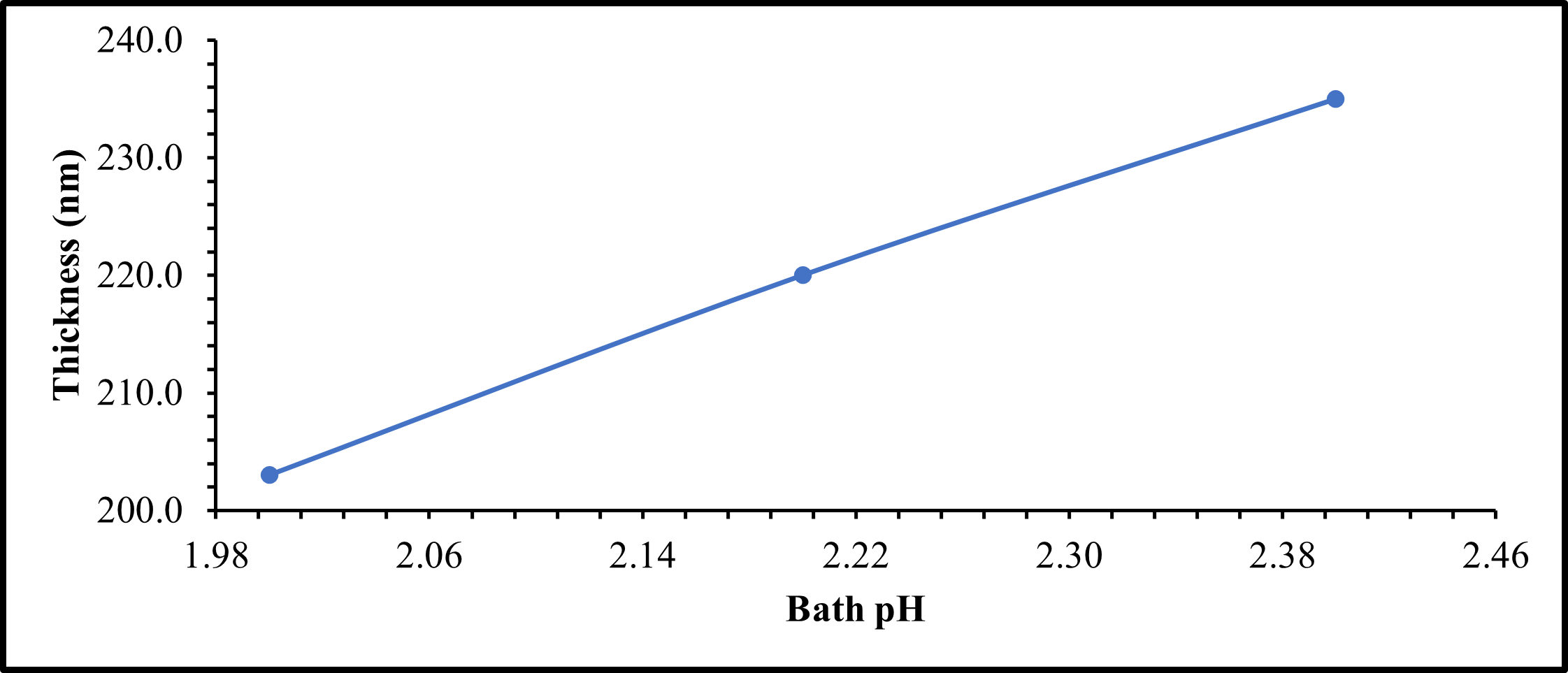
Figure 1: The graph of the CuSe thickness against bath pH
PHOTOELECTROCHEMICAL (PEC) CELL MEASUREMENT STUDY
Figure2, illustrates the PEC cell signal for CuSe thin films at their various bath pH. The PEC cell signals show that samples of CuSe layers grown at pH 2.0, 2.2 and 2.4 are p-type in electrical conduction. The results also shows that a pH of 2.2 has the highest PEC cell signal. This indicates that the CuSe thin film exhibits the highest conductivity at this highest PEC cell signal.
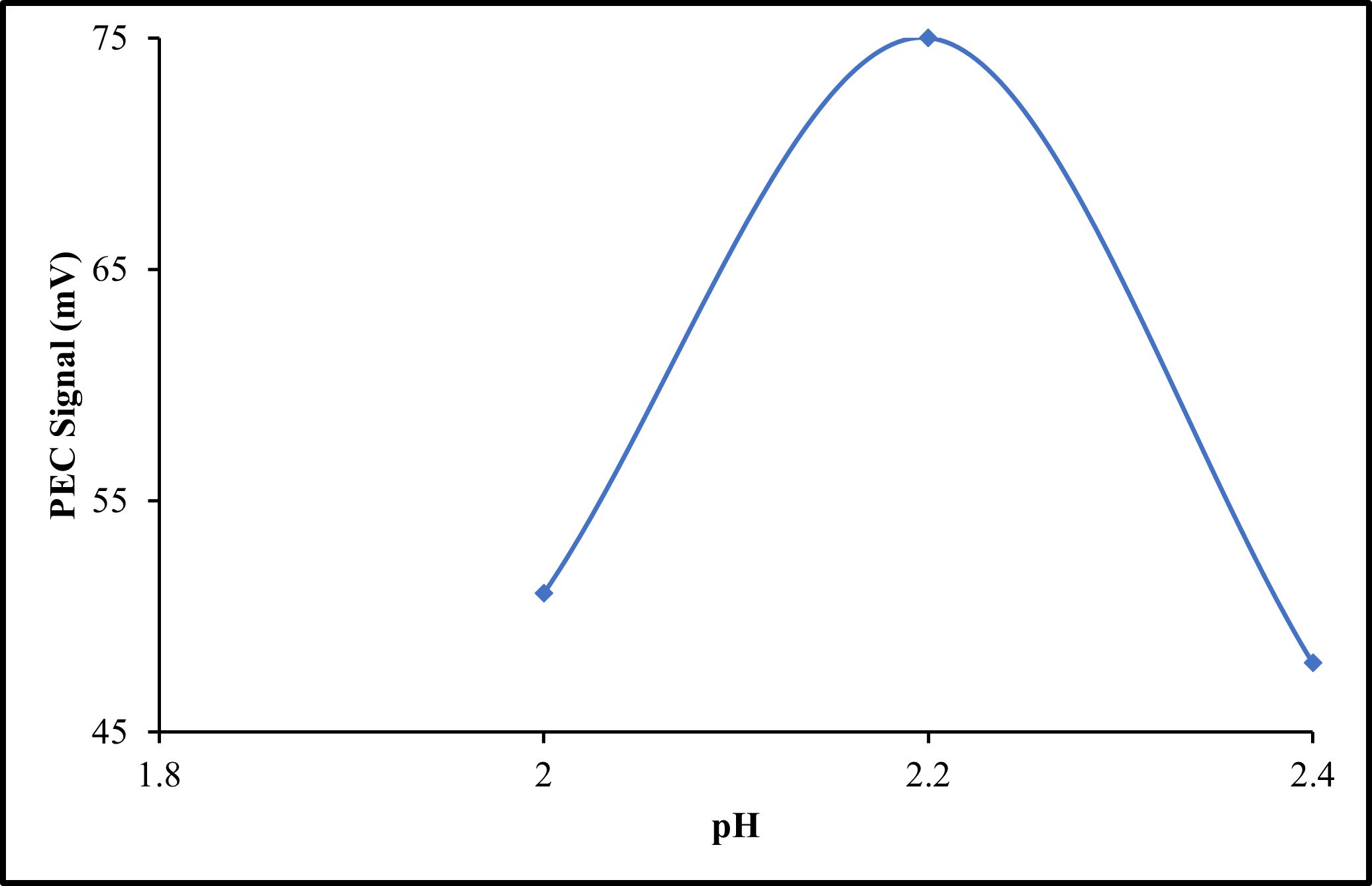
Figure 2: Typical PEC cell signals for CuSe at the different bath pH
Effect of pH variation on photo-conductivity of CuSe thin films
Photoconductivity is due to the absorption of photons, which leads to the creation of free charge carriers in the conduction band and the valence band. It provides valuable information about the physical properties of materials and offers applications in photodetection and radiation measurements. The photo responses of CuSe thin films under dark and light conditions are illustrated in Figures 3 and Figure 4. Figure 3 illustrates the variation of resistance of CuSe layers under dark and illuminated conditions at varying electrolytic bath pH. The results indicated that all the CuSe thin films electroplated within the explored pH range have resistance lesser than 50.0 Ω. This is a good indication since low-resistance semiconductors are suitable for optoelectronic applications, especially in solar cell fabrication.
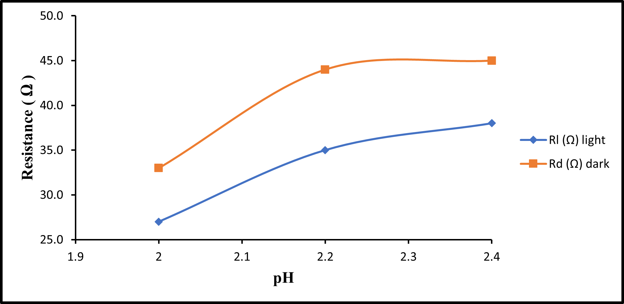
Figure 3 Variation of resistance of CuSe thin film layers under dark and light condition at varying bath pH
As seen in Figure 3, CuSe thin films have higher resistance values in the dark compared to the observed values in light. It is generally known that it is a typical characteristic of a semiconductor to possess higher resistance in the dark and lesser resistance values in the light. This is because there are no photon absorptions by the semiconductors under dark conditions, whereas in light or illuminated condition, semiconductors absorb photons. The photon absorption leads to the excitation of electrons from the valence band to the conduction band, thus creating electron-hole pairs (charge carriers). The presence of more conduction electrons within the conduction band improves the material’s electrical conductivity. Thus, an improvement in the material’s conductivity lowers the material’s resistance as observed in Figure 3. Also, the maximum photocurrent (ILmax) observed in CuSe layers electrodeposited at pH of 2.0, 2.2 and 2.4 are 1.0, 2.0 and 1.4 mA respectively. The values observed for the maximum dark current (IDmax) are 0.4, 1.2 and 0.9 mA for CuSe films grown at pH of 2.0, 2.2 and 2.4, respectively. Overall, the observed photocurrent is higher than the dark current at the respective pH values as shown in Table 1. The higher photocurrent under illumination is a possible reason for lower resistance values observed in light conditions, as seen in Figure 3. The higher photocurrent can be mainly attributed to the generation of mobile charge carriers caused by photon absorption.
Table 1: The observed photocurrent in CuSe thin film layers
| pH | Light ILmax | Dark IDmax |
| 2.0 | 1.0 | 0.4 |
| 2.2 | 2.0 | 1.2 |
| 2.4 | 1.4 | 0.9 |
The higher photocurrent also leads to the generation of higher maximum power (Pmax) under illumination conditions; thus is illustrated in Figure 4. Figure 4 thus shows that CuSe layers have higher maximum power under illumination conditions, with the highest value observed at the materials grown at a pH of 2.2. As previously stated, CuSe materials grown at a pH of 2.2 also have the highest photo and dark currents. The result, therefore, shows the direct relationship between maximum current and power. Since the photocurrent of the CuSe layer is more than the dark current, The electrodeposited CuSe is said to exhibit positive photoconductivity. The positive photoconductivity is due to the generation of mobile charge carriers caused by the absorption of photons.
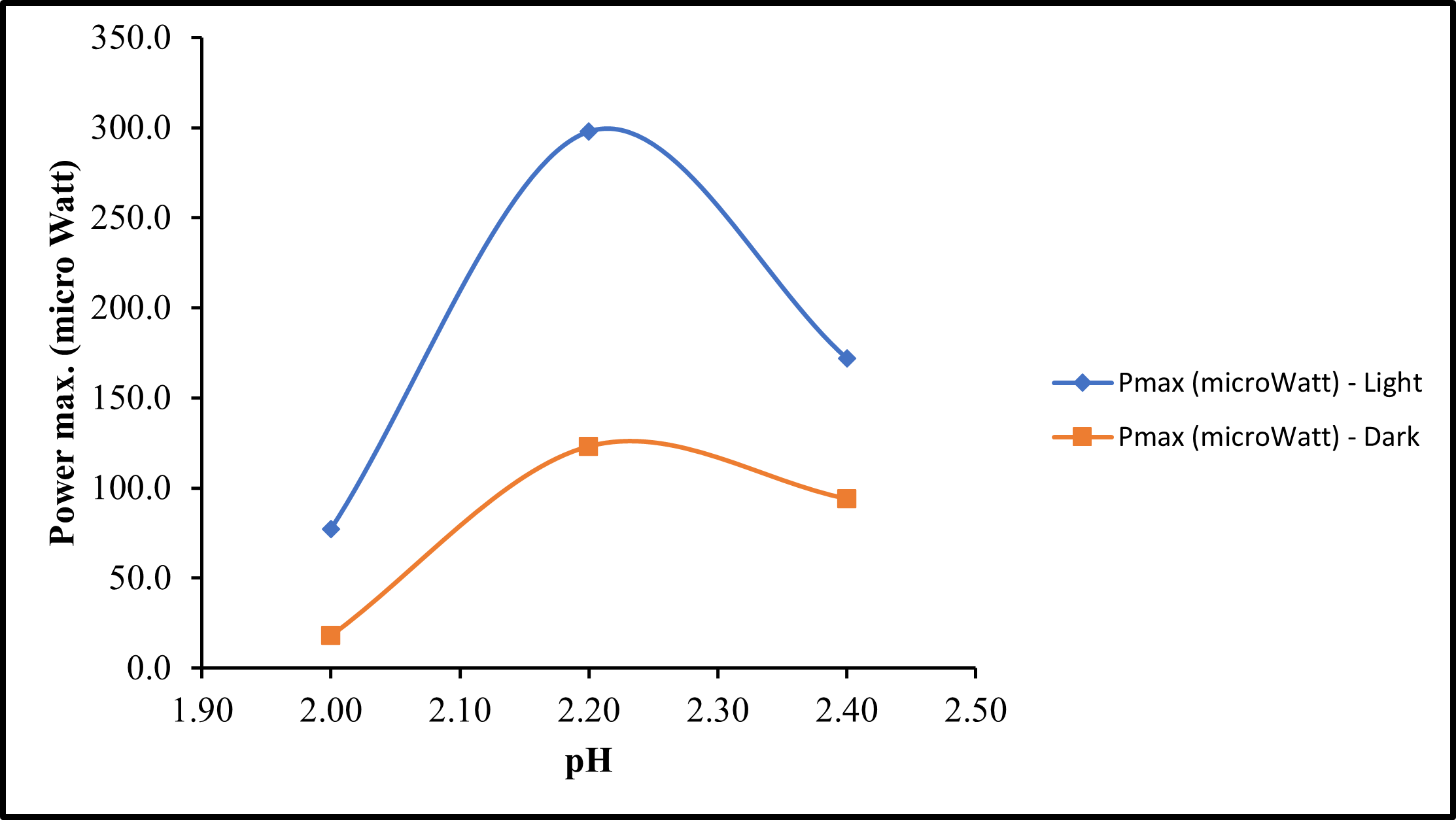
Figure 4: Variation of power of CuSe thin film layers under dark and light condition at varying bath pH
EFFECT OF PH VARIATION ON THE OPTICAL PROPERTIES OF CUSE THIN FILMS
Optical properties are important as far as optoelectronic device applications are concerned. Optical absorbance, transmittance, and band gap of CuSe thin film layers are to be considered in this research study. The optical absorbance and transmittance spectra of CuSe thin film layers are recorded in the wavelength region 350 nm to 900 nm; these are illustrated in Figure 5 and Figure 6, respectively.
Optical Absorption Study
In this study, a UV-VIS spectrophotometer was used to measure the optical absorption of CuSe thin film. Figure 5 shows the optical absorption spectra for the selected pH values. The optical absorbance of CuSe semiconductor has its highest values at the ultraviolet region ( λ < 400 nm ) and gradually decreases along the visible region ( 400 nm -700 nm ). At the same time, it starts to increase along the infrared region ( λ > 700 nm ).
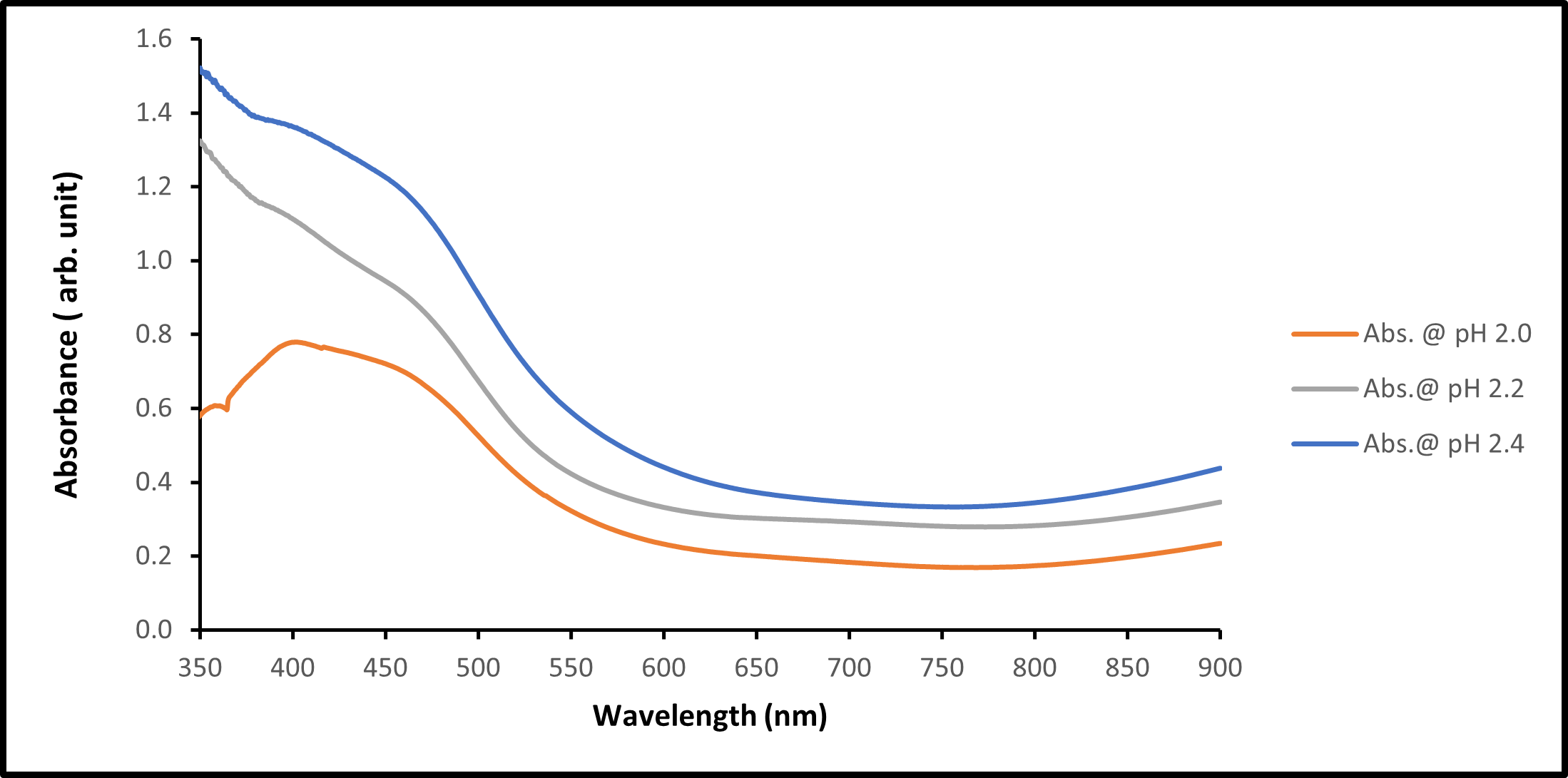
Figure 5: Graph of absorbance against wavelength at pH 2.00, 2.20 and 2.40
As illustrated in Figure 5, the absorbance of the CuSe semiconductors increases as pH increases. The increase in pH results in the rate at which the materials absorb photons from the solar spectrum. The absorbance of CuSe at pH of 2.0 has the least, while that of 2.40 possesses the highest level of absorbance. Because CuSe thin films have their highest absorbance at both ultraviolet and visible regions (350 nm to 450 nm), it makes them appropriate for photovoltaic applications.
Optical Transmittance Study
The transmittance of CuSe thin film layers was obtained by using UV-VIS spectrophotometer. Figure6, illustrates the optical transmittance spectra for electrodeposited CuSe thin film layers at pH 2.00, 2.20 and 2.40. As shown in Figure 6, the thin film layers started transmitting within the ultraviolet region (λ ˂ 400 nm) and increased with an increase in the wavelength up to the infrared region (λ ˃ 700 nm ). The CuSe thin films attained high transmission peaks in the infrared region; this features makes CuSe thin film semiconductor a suitable material to use as a high-power infrared sensor (Petrović et al., 2017). The least transmittance of CuSe was recorded at a pH of 2.4 while the highest transmittance value was recorded at pH of 2.0.
![]()
Figure 6: The optical transmittance spectra for electrodeposited CuSe thin film layers at pH of 2.00, 2.20 and 2.40.
Optical Band-gap Study
The plot of (αhν)2 versus (hν) for CuSe thin films at pH of 2.00, 2.20 and 2.40 obtained at optimized condition is shown in Figure 7. Extrapolation of linear portion of the graph to the photon energy (hν) axis at (αhν)2 = 0 gives band gap energy of the material. The band gap values of the electrodeposited films were found to be 2.30 eV, 2.20 eV and 2.00 eV at bath pH of 2.0, 2.2.and 2.4 respectively. The optical band obtained at these various pH tends to decrease as pH increases.The obtained band gap values agree with the bulk band gap of CuSe (Sadekar 2018).

Figure 7: The optical band-gap for electrodeposited CuSe thin film layers at pH of 2.00, 2.20 and 2.40.
Table2, illustrates the optical parameters obtained from electrodeposited CuSe thin films at pH of 2.0, 2.2 and 2.4. The optical parameters shown in Table 2 at each pH variations were; the average thickness (T), energy band gap (Eg), the average refractive index (navg), average absorption coefficient ( αavg ), average extinction coefficient (kavg), average total dielectrics (ET) which is the addition of both real and imaginary dielectrics, average optical conductivity(σavg), average absorbance (Aavg), average transmittance (Tavg) and average reflectance (Ravg).
| T (nm) | Eg (eV) | navg | αavg (cm-1) | kavg | σavg (s-1) | ET | AAVG | TAVG | RAVG | A+T+R | |
| 2.0 | 203.0 | 2.30 | 2.29 | 37050.62 | 0.16 | 2.08 | 6.04 | 0.36 | 0.49 | 0.15 | 1 |
| 2.2 | 220.0 | 2.20 | 2.52 | 57652.26 | 0.24 | 2.23 | 7.37 | 0.52 | 0.37 | 0.11 | 1 |
| 2.4 | 235.0 | 2.00 | 2.53 | 67585.81 | 0.28 | 2.44 | 7.54 | 0.66 | 0.30 | 0.04 | 1 |
Table 2: The optical parameters obtained from electrodeposited CuSe thin films of different pH values
As seen in Table 2, band gap energy, transmittance and reflectance decrease as pH increases while the remaining optical parameters like thickness, refractive index, absorption coefficient, extinction coefficient, optical conductivity, total dielectrics and absorbance of the CuSe thin films increase as pH increases. The summation of the average absorbance (A), transmittance (T), and reflectance (R), in the table endorses the law of conservation of energy which makes the summation of the trio in the CuSe thin films equal to one as seen in the table. The average absorbance shows that high absorbance value observed in the CuSe grown at pH of 2.40 will make the films appropriate as photo absorbers in solar cell fabrication (Nwofe et al., 2017).
X-RAY DIFFRACTION STUDIES OF CUSE THIN FILMS LAYERS
CuSe layers exist in different structural phases such as Bellidorite (Cu2Se), Klockmannite (CuSe). The x-ray diffraction is a characterisation technique that helps in distinguishing the type of structural phases that exist in the electrodeposited layers. As seen in this work, the preferred orientation peak of electrodeposited CuSe layers exists as klockmannite (CuSe) and this corresponds to reference code 00-006-0427. The position in which these klockmannite phases occurred ranges from 2θ = 26.727o to 26. 756o within the bath pH values explored in this work. The XRD spectra of the electrodeposited CuSe layers are shown in Figure 8. The preferred orientation peak was observed at specific positions of 2θ = 26.7311o, 26.7562o, and 26.7266o for CuSe layers grown at bath pH of 2.00, 2.20 and 2.40 respectively. These positions (angles) combined with their respective full width at half maximum (FWHM or β ) values given in Table 3 were used in estimating the crystallite sizes (D) of the electrodeposited layers according to Scherrer’s formula given in equation 1.
![]() 1
1
The λ is the wavelength of the Cu-Kα monochromator of the Rigaku diffractometer; the wavelength has a value of 1.542 Å. The estimated crystallite sizes of electrodeposited CuSe at bath pH values of 2.00, 2.20 and 2.40 are approximately 37.83 nm, 76.68 nm and 50.32 nm respectively. The highest peak intensity for the preferred orientation peak occurred at pH of 2.20. at this pH value, the electrodeposited CuSe layers have the highest crystallite sizes as revealed in Figure 9
Table 3: Some structural parameters of ED-CuSe layers obtained at pH of 2.00, 2.20 and 2.40.
| pH | Position (2θ) | Heights (cts) | FWHM (2θ ) | D-Spacing [A0 ] |
| 2.00 | 26.7311 | 32.98 | 0.3149 | 3.33504 |
| 34.1021 | 11.51 | 0.4723 | 2.62918 | |
| 37.9724 | 66.47 | 0.1574 | 2.36963 | |
| 51.7256 | 20.21 | 0.3149 | 1.76732 | |
| 61.8667 | 7.57 | 0.9446 | 1.49976 | |
| 65.6778 | 13.20 | 0.4723 | 1.42166 | |
| 2.20 | 26.7562 | 81.12 | 0.1574 | 3.33196 |
| 33.9841 | 29.26 | 0.2362 | 2.63804 | |
| 37.9920 | 52.38 | 0.1968 | 2.36845 | |
| 51.7288 | 69.15 | 0.2362 | 1.76722 | |
| 65.7611 | 26.14 | 0.4723 | 1.42006 | |
| 2.40 | 26.7266 | 50.24 | 0.2362 | 3.33559 |
| 33.9475 | 26.31 | 0.3149 | 2.64080 | |
| 37.8799 | 44.39 | 0.2755 | 2.37520 | |
| 51.6907 | 65.48 | 0.1968 | 1.76843 | |
| 61.8006 | 9.94 | 0.4723 | 1.50120 | |
| 65.7188 | 24.39 | 0.3936 | 1.42087 |
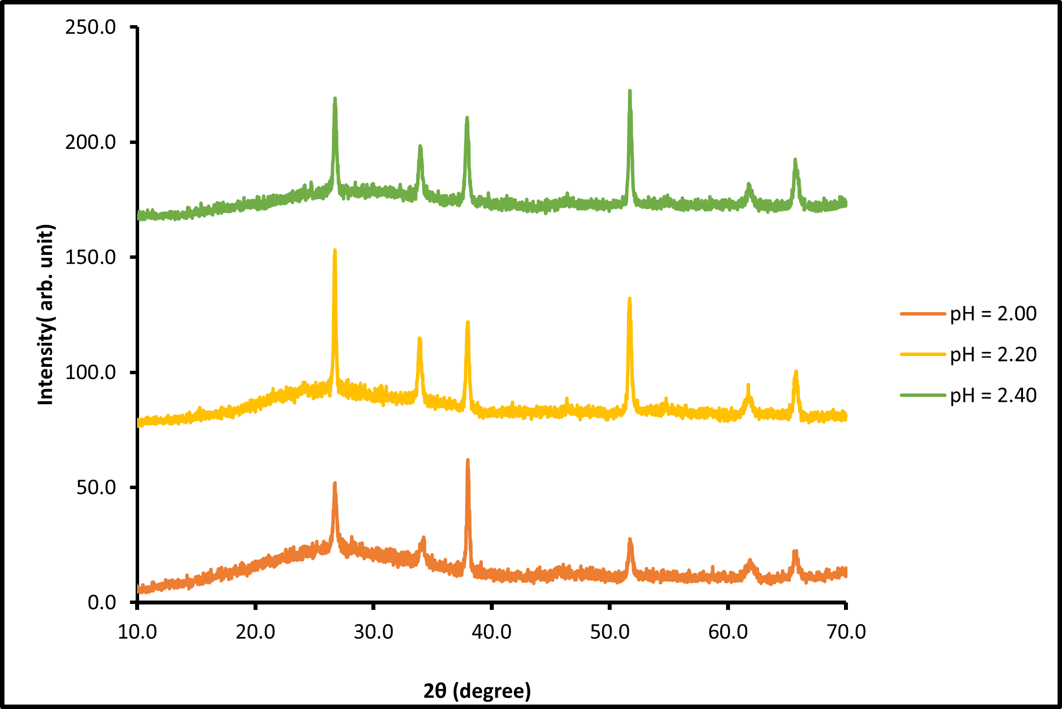
Figure 8: The XRD spectra of electrodeposited CuSe layers grown at pH of 2.00, 2.20 and 2.40
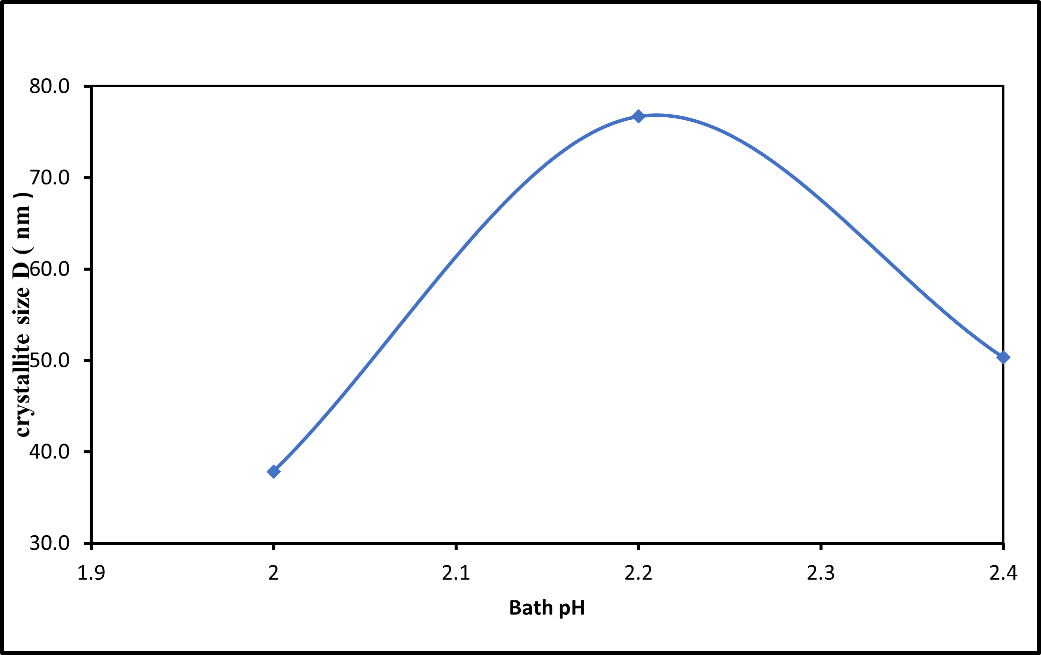
Figure. 9: The crystallite sizes of electrodeposited CuSe layers grown at pH of 2.00, 2.20 and 2.40
CONCLUSION
The effect of pH variation on the optoelectronic and structural properties of electrodeposited copper selenide thin films has been Investigated and the research revealed that the resistance of the thin film semiconductor is always higher in the dark than in the light. and both the photo and the dark current of CuSe thin films increase linearly with the bath pH thus photo current is more than the dark current. Also, the increase in bath pH results to the rate at which the absorbance started to be absorbed. with the decrease in the band gap of CuSe thin films as its grown bath pH increases The preferred orientation peak of electrodeposited CuSe layers exists as klockmannite (CuSe) and this corresponds to reference code 00-006-0427. The position in which these klockmannite phases occurred ranges between 2θ = 26.727o to 26. 7560 within the bath pH values explored.
ACKNOWLEDGEMENT
I acknowledge the efforts of the following in making this research a success; the Condensed Matter Laboratory of The Federal University of Technology Akure where the electrodeposition process and sample characterisation took place. Also, I appreciated Dr. O. I. Olusola for his guidance during the research work in the laboratory and reading through the paper for correction purpose.
REFERENCES
- Boolchandani, S., Srivastava, S., & Vijay, Y. K. (2018). Preparation of InSe Thin Films by Thermal Evaporation Method and Their Characterization: Structural, Optical, and Thermoelectrical Properties. Journal of Nanotechnology, 2018, 1-9.
- Ezenwa, I. A., Okereke, N. A., & Okoli, L. N. (2013). Optical Properties of Copper Selenide Thin Film. International Research Journal of Engineering Science, Technology and Innovation (IRJESTI) 2(5), 82–87.
- Gromboni, M. F., & Mascaro, L. H. (2016). Optical and structural study of electrodeposited zinc selenide thin films. Journal of Electroanalytical Chemistry, 780, 360–366.
- Guerrero, L., & Nair, P. K. (1999). Effect of thermal processing on optical and electrical properties of copper selenide thin films. 213–218.
- Islam, A. B. M. O., & Bhuiyan, A. H. (2005). Structural , electrical and optical properties of copper selenide thin films deposited by chemical bath deposition technique. 6, 2–3.
- Nwofe, P. A., Chikwenze, R. A., Agbo, P. E., & Igwe, H. U. (2017). Deposition and characterization of nickel selenide thin films for applications in optoelectronic devices. Asian Journal of Scientific Research, 10(1), 43–49. https://doi.org/10.3923/ajsr.2017.43.49
- Petrović, M., Gilić, M., Ćirković, J., Romčević, M., Romčević, N., Trajić, J., & Yahia, I. (2017). Optical properties of CuSe thin films – band gap determination. Science of Sintering, 49(2). https://doi.org/10.2298/SOS1702167P
- Qasrawi, A. F., & Rob, O. H. . (2019). Effect of insertion of Aluminium nanosheets on the structural , optical and dielectric properties of stacked layers of Selenium. Chalcogenide 16(6), 257–263.
- Ramesh, K., Thanikaikarasan, S., & Bharathi, B. (2014). Structural , Morphological and Optical Properties of Copper Selenide Thin Films. International Journal of ChemTech Research. 6(13), 5408–5411.
- Sadekar Harishchandra K. (2018). Optical and Structural Properties of CuSe Thin Films Deposited by Chemical Bath Deposition ( CBD ) Technique. International Research Journal of Science and Engineering; Special Issue A2, 20–22.
- Sandoval-Paz, M. G., Rodríguez, C. A., Porcile-Saavedra, P. F., & Trejo-Cruz, C. (2016). Study of the crystallographic phase change on copper (I) selenide thin films prepared through chemical bath deposition by varying the pH of the solution. Journal of Solid State Chemistry, 239.